Institute of Engineering Education Special lectures
— Semiconductor Market and Related Technologies —
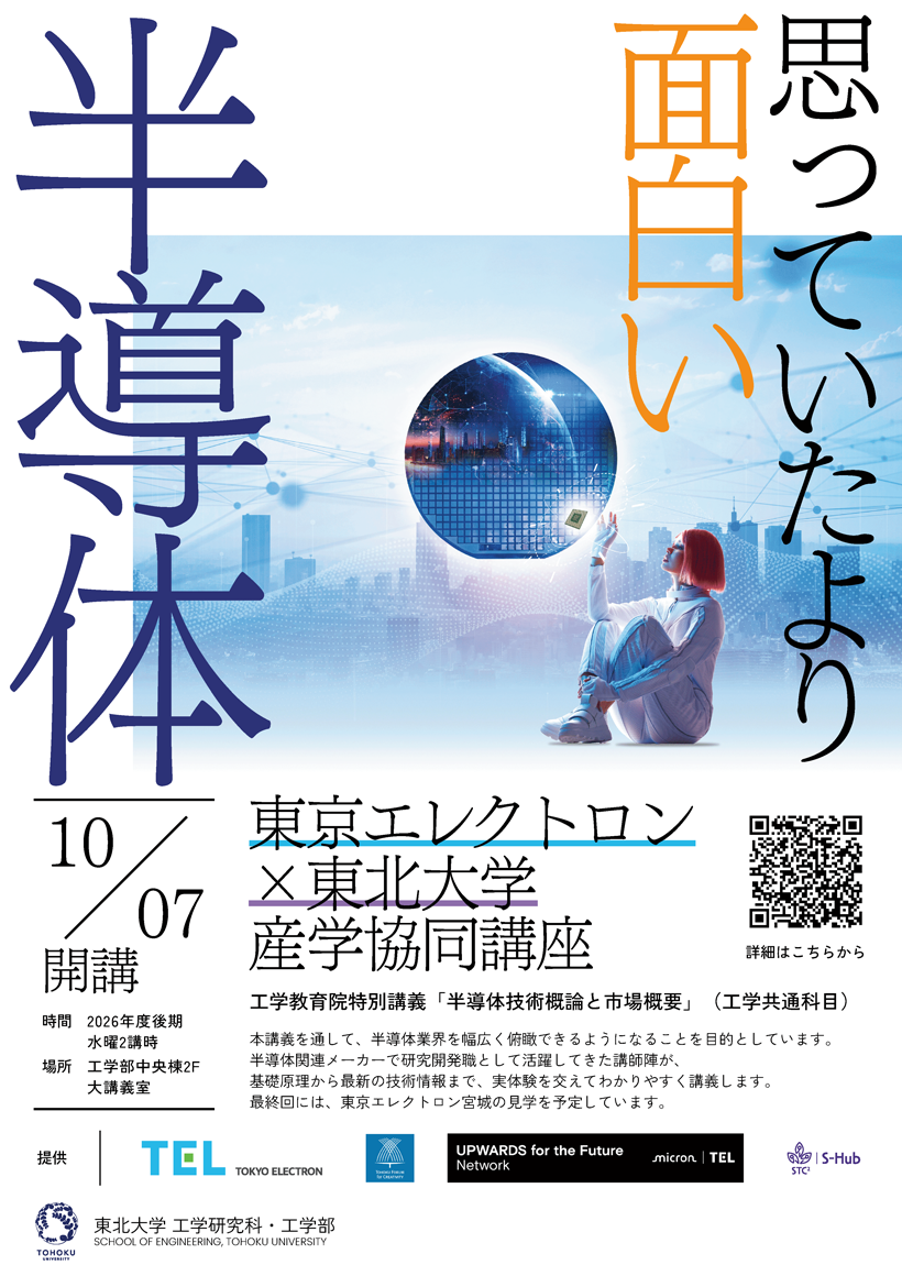
Information
Date
Wednesday, October 7, 2026 – Early February 2027
Venue
Large Lecture Hall, Center Building 2F (C01), Faculty of Engineering, Aobayama Campus, Tohoku University [Access]
Link
https://qsl.cds.tohoku.ac.jp/syllabus/display/tm85105300–2026
*Students who wish to enroll in the course should register for the course.
Course Objectives and Summary / Learning Goals
This course aims to develop professionals who can gain a broad and comprehensive perspective on the semiconductor industry.
Semiconductors are a foundational technology for nearly all modern industries and encompass a wide range of technological fields. The semiconductor market is also diverse and continues to evolve rapidly.
Through this course, students will learn the fundamental technologies that make up the semiconductor technical value chain, including basic physical principles, materials, design, manufacturing equipment, facilities, manufacturing processes, characterization, and analysis. Students will also study the structure and dynamics of the semiconductor market.
The course aims to equip students with the knowledge and perspective needed to contribute not only to semiconductor manufacturers, but also to a wide range of industries and markets related to semiconductor technologies.
Learning goals are:
- To gain a comprehensive understanding of the roles, significance, and fundamental technologies associated with each stage of the semiconductor technical value chain.
- To develop a broader understanding of how one's own field of expertise relates to and integrates with surrounding technical disciplines.
Course Description
This course consists of 13 lectures and one comprehensive understanding test. The 15th session will be a facility visit to a semiconductor manufacturing equipment manufacturer, scheduled for early February 2027.
Time Schedule
- Wednesday, October 7, 2026
- 10:30 – 12:00
- Lecture 1: Global Semiconductor Market Trends
- An overview of the global semiconductor ecosystem, covering products, materials, equipment, and design automation, while exploring the intersection with social trends—including SDGs (Sustainable Development Goals)
- Wednesday, October 14, 2026
- 10:30 – 12:00
- Lecture 2: Semiconductor Materials and Physical Properties
- Foundations of materials (semiconductors, insulators, and conductors), electronic components (R, C, Diode, MOS), and the fundamentals of energy band diagrams.
- Wednesday, October 21, 2026
- 10:30 – 12:00
- Lecture 3: Nano-level Process Technology (Front-end)
- Fundamental principles of front-end-of-line (FEOL) processes: Lithography, Deposition, Dry Etching, CMP (Chemical Mechanical Planarization), and Cleaning/Drying.
- Wednesday, October 28, 2026
- 10:30 – 12:00
- Lecture 4: Advanced CMOS Device Technology
- The evolution of MOSFET architecture: Learning the structure, fabrication methods, and operation of Planar, FinFET, and GAA (Gate-All-Around) FETs.
- Wednesday, November 4, 2026
- 10:30 – 12:00
- Lecture 5: AI Memory Technologies
- Structure, manufacturing, and operation of advanced memory: Advanced DRAM (HBM - High Bandwidth Memory), 3D NAND Flash, and non-volatile memory MRAM.
- Wednesday, November 11, 2026
- 10:30 – 12:00
- Lecture 6: Structure and Dynamics of the Semiconductor Equipment Market
- Analysis of the semiconductor manufacturing equipment (SME) market and the strategic challenges faced by major equipment manufacturers.
- Wednesday, November 18, 2026
- 10:30 – 12:00
- Lecture 7: Introduction to Advanced Manufacturing Systems
- A deep dive into semiconductor manufacturing equipment and the cutting-edge technologies in lithography-related spin-coating/developing, and cleaning processes.
- Wednesday, November 25, 2026
- 10:30 – 12:00
- Lecture 8: Cutting-edge Plasma Process Technology
- The forefront of microfabrication: Exploring advanced plasma etching techniques for ultra-fine circuit patterns.
- Wednesday, December 2, 2026
- 10:30 – 12:00
- Lecture 9: 3D and Nano-level Deposition
- The latest advancements in thin-film deposition technologies, focusing on atomic-scale control and 3D structures.
- Wednesday, December 16, 2026
- 10:30 – 12:00
- Lecture 10: AI Processor Design
- A comprehensive look at circuit design: Basic circuits, LSI design, SPICE simulation, SoC (System on Chip) architecture, and the design of CPUs, GPUs, and AI-specific processors.
- Wednesday, December 23, 2026
- 10:30 – 12:00
- Lecture 11: Power Devices and Image Sensors
- Structure and operation of various power semiconductors, alongside the architecture, manufacturing, and physics of CIS (CMOS Image Sensors).
- Wednesday, January 6, 2027
- 10:30 – 12:00
- Lecture 12: Advanced Packaging (Back-end)
- Back-end-of-line (BEOL) processes: Advanced packaging technologies, dicing, bonding, and molding.
- Wednesday, January 13, 2027
- 10:30 – 12:00
- Lecture 13: Product Yield and Quality Control
- Foundations of electrical characterization, yield management, reliability testing, failure analysis, and physical analysis.
- Wednesday, January 20 or 27, 2027
- 10:30 – 12:00
- Lecture 14: Course Summary and comprehensive understanding examination
- Early February 2027
- TBA
- Lecture 15: Facility Visit to a Semiconductor Equipment Manufacturer
- A field trip to observe the technologies learned in class firsthand, gaining a practical sense of scale and industrial application.
Poster
- Download [PDF]
Co–hosted by
- Tokyo Electron Limited
- Tohoku Forum for Creativity, Tohoku University
- UPWARDS for the Future
- Semiconductor Creativity Hub (S–Hub), Tohoku University
Contact
Email: tfc_co*grp.tohoku.ac.jp (change * to @)